
ABSTRACT
In this project, two high performance adder cells are proposed. We simulated these two full adder cells using HSPICE in 0.18 µm, CMOS technology and at 25-degree of temperature with supply voltage range from 0.5v to 3.3v with 0.1v steps. Results show that the proposed adders operate successfully when connected to a 0.5 V power supply. The two adders differ in the technology applied to their gates. While the first circuit applies CMOS technology, the second and optimal one uses Past Transistor Logic. The average power dissipation of the optimum is 4.3269*10-7 watt, which illustrates an amazing performance. This paper demonstrates the PDP and Power Consumption of the proposed adders, and the comparison results among another six full adders.
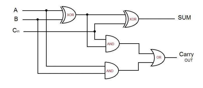
Image source: Theorycircuit.com
Copyright © 2023 Author(s) retain the copyright of this article.
This article is published under the terms of the Creative Commons Attribution License 4.0
If you like this article, see others like it:
- Optimization of Battery Management System (BMS) for Nanosatellite
- Development of Software for Life Cycle Cost Analysis of Solar Photovoltaic and Diesel Generator Systems in Nigeria
- Design and Construction of 1.5 KVA Inverter
- Construction of Step Up Transformer with Multi-Output
- Construction of Battery Charge Control for Photovoltaic Systems